logo

Loading...
  • Home
  • Categories
  • Manufacturers
  • Products
  • PROJECTS
  • TUTORIAL
  • CODE LIBRARY
  • Blogs
  • Contact us
  1. Home
  2. Product Categories
  3. Components & IC's
  4. OPAMP
  5. AD711 BiFET Opamp
AD711 BiFET Opamp
*Images are shown only for references
AD711 BiFET Opamp

Description

AD711 BiFET Opamp

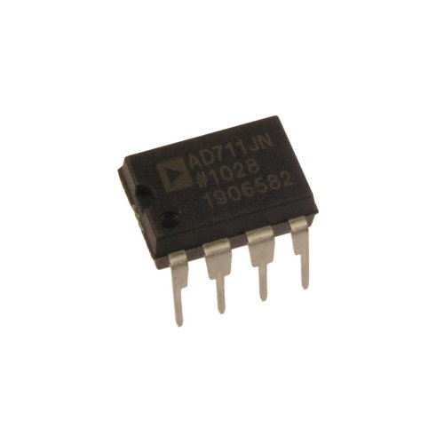
AD711 Low Cost BiFET OPAMP
The AD711 is a high speed, precision monolithic operational amplifier offering high performance at very modest prices. Its very low offset voltage and offset voltage drift are the results of advanced laser wafer trimming technology. These performance benefits allow the user to easily upgrade existing designs that use older precision BiFETs and, in many cases, bipolar op amps.

The superior ac and dc performance of this op amp makes it suitable for active filter applications. With a slew rate of 16 V/µs and a settling time of 1 µs to ±0.01%, the AD711 is ideal as a buffer for 12-bit D/A and A/D Converters and as a high-speed integrator. The settling time is unmatched by any similar IC amplifier.

The combination of excellent noise performance and low input current also make the AD711 useful for photo diode preamps. Common-mode rejection of 88 dB and open loop gain of 400 V/mV ensure 12-bit performance even in high-speed unity gain buffer circuits.

HIGHLIGHTS of AD711

  • The AD711 offers excellent overall performance at very competitive prices.
  • Analog Devices’ advanced processing technology and 100% testing guarantee a low input offset voltage (0.25 mV max, C grade, 2 mV max, J grade). Input offset voltage is specified in the warmed-up condition. Analog Devices’ laser wafer drift trimming process reduces input offset voltage drifts to 3 mV/∞C max on the AD711C.
  • Along with precision dc performance, the AD711 offers excellent dynamic response. It settles to ±0.01% in 1 ms and has a 100% tested minimum slew rate of 16 V/ms. Thus this device is ideal for applications such as DAC and ADC buffers which require a combination of superior ac and dc performance.
  • The AD711 has a guaranteed and tested maximum voltage noise of 4 mV p-p, 0.1 to 10 Hz (AD711C).
  • Analog Devices’ well-matched, ion-implanted JFETs ensure a guaranteed input bias current (at either input) of 25 pA max (AD711C) and an input offset current of 10 pA max (AD711C). Both input bias current and input offset current are guaranteed in the warmed-up condition.

Features of AD711 BiFET OPAMP

  • Enhanced Replacement for LF411 and TL081
  • AC PERFORMANCE
  1. Settles to 0.01% in 1.0 s
  2. 16 V/s min Slew Rate (AD711J)
  3. 3 MHz min Unity Gain Bandwidth (AD711J)
  • DC PERFORMANCE
  1. 0.25 mV max Offset Voltage: (AD711C)
  2. 3 V/C max Drift: (AD711C)
  3. 200 V/mV min Open-Loop Gain (AD711K)
  4. 4 V p-p max Noise, 0.1 Hz to 10 Hz (AD711C)
  • Available in Plastic Mini-DIP, Plastic SOIC, HermeticCerdip, and Hermetic Metal Can Packages

Related Link

  • Download AD711 BiFET Opamp Datasheet

AD711 BiFET Opamp

4

See 1 Ratings & Reviews |

Stock: 5
SKU: DAA013

₹ 365.80  (inc GST)

Description

AD711 BiFET Opamp

AD711 Low Cost BiFET OPAMP
The AD711 is a high speed, precision monolithic operational amplifier offering high performance at very modest prices. Its very low offset voltage and offset voltage drift are the results of advanced laser wafer trimming technology. These performance benefits allow the user to easily upgrade existing designs that use older precision BiFETs and, in many cases, bipolar op amps.

The superior ac and dc performance of this op amp makes it suitable for active filter applications. With a slew rate of 16 V/µs and a settling time of 1 µs to ±0.01%, the AD711 is ideal as a buffer for 12-bit D/A and A/D Converters and as a high-speed integrator. The settling time is unmatched by any similar IC amplifier.

The combination of excellent noise performance and low input current also make the AD711 useful for photo diode preamps. Common-mode rejection of 88 dB and open loop gain of 400 V/mV ensure 12-bit performance even in high-speed unity gain buffer circuits.

HIGHLIGHTS of AD711

  • The AD711 offers excellent overall performance at very competitive prices.
  • Analog Devices’ advanced processing technology and 100% testing guarantee a low input offset voltage (0.25 mV max, C grade, 2 mV max, J grade). Input offset voltage is specified in the warmed-up condition. Analog Devices’ laser wafer drift trimming process reduces input offset voltage drifts to 3 mV/∞C max on the AD711C.
  • Along with precision dc performance, the AD711 offers excellent dynamic response. It settles to ±0.01% in 1 ms and has a 100% tested minimum slew rate of 16 V/ms. Thus this device is ideal for applications such as DAC and ADC buffers which require a combination of superior ac and dc performance.
  • The AD711 has a guaranteed and tested maximum voltage noise of 4 mV p-p, 0.1 to 10 Hz (AD711C).
  • Analog Devices’ well-matched, ion-implanted JFETs ensure a guaranteed input bias current (at either input) of 25 pA max (AD711C) and an input offset current of 10 pA max (AD711C). Both input bias current and input offset current are guaranteed in the warmed-up condition.

Features of AD711 BiFET OPAMP

  • Enhanced Replacement for LF411 and TL081
  • AC PERFORMANCE
  1. Settles to 0.01% in 1.0 s
  2. 16 V/s min Slew Rate (AD711J)
  3. 3 MHz min Unity Gain Bandwidth (AD711J)
  • DC PERFORMANCE
  1. 0.25 mV max Offset Voltage: (AD711C)
  2. 3 V/C max Drift: (AD711C)
  3. 200 V/mV min Open-Loop Gain (AD711K)
  4. 4 V p-p max Noise, 0.1 Hz to 10 Hz (AD711C)
  • Available in Plastic Mini-DIP, Plastic SOIC, HermeticCerdip, and Hermetic Metal Can Packages

Related Link
  • Download AD711 BiFET Opamp Datasheet

newsletter image

Join our mailing list

Get bits and bytes of noise free Information

*No Noise(spam) only Information

Get In Touch

Office

DNA Solutions, Flat no 1, Raja Jeet Recidency, p no 61 Sr no 102, Wadala Shivar Indira nagar, Nashik, 422009, Maharashtra, India

Shop

FH11-12, Thakker Bazar NEW CBS, Nashik, 422002, Maharashtra, India

Got Questions? Call us at

Neha (Rest of India): 7972667515, 8412906903

Prachi (Nashik): 8669102120

site@example.com

Information

  • FAQs
  • About Us
  • Shipping & Delivery
  • Returns & Cancellation
  • Privacy Policy
  • Payment Information
  • Terms & Conditions
  • Contact us
  • Products
  • Blogs
Cities Cover

Shivaji Nagar | Namrup | Thane | Pilani | Ballia | Darbhanga | Kannur | Junagadh | Jaisalmer | Jamshedpur | Itanagar | Amravati | Navi Mumbai | Durgapur | Dahod | Pimpri | Madurai | Agra | Mangalore | Kalyan | Port Blair | Davangere | Kochi | Pondicherry | Mathura | Kalyan | Raigad | Thane | Nagpur | Bhubaneswar

COPYRIGHT © 2026 DNA Solutions, INDIA . ALL RIGHTS RESERVED.

footer-logos