
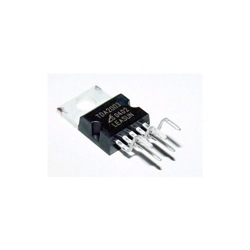
The UTC TDA2030 is a monolithic audio power amplifier integrated circuit.
TDA2030 is 18 watt Hi-Fi Audio Amplifier. The TDA2030 Audio amplifier provides high output current and has very low harmonic and cross-over distortion. Further the device incorporates a short circuit protection system comprising an arrangement for automatically limiting the dissipated power so as to keep the working point of the output transistors within their safe operating area. A conventional thermal shut-down system is also included.
Very low external component required.
High current output and high operating voltage.
Low harmonic and crossover distortion.
Built-in Over temperature protection.
Short circuit protection between all pins.
Safety Operating Area for output transistors.
Supply Voltage Vs : ±18 V
Input Voltage VIN : Vs V
Differential Input Voltage VI(DIFF) : ±15 V
Peak Output Current(internally limited) I OUT : 3.5 A
Total Power Dissipation at Tc=90°C PD : 20 W
Junction Temperature TJ : -40~+150 °C
Storage Temperature TSTG : -40~+150 °C
See 0 Ratings & Reviews |
The UTC TDA2030 is a monolithic audio power amplifier integrated circuit.
TDA2030 is 18 watt Hi-Fi Audio Amplifier. The TDA2030 Audio amplifier provides high output current and has very low harmonic and cross-over distortion. Further the device incorporates a short circuit protection system comprising an arrangement for automatically limiting the dissipated power so as to keep the working point of the output transistors within their safe operating area. A conventional thermal shut-down system is also included.
Very low external component required.
High current output and high operating voltage.
Low harmonic and crossover distortion.
Built-in Over temperature protection.
Short circuit protection between all pins.
Safety Operating Area for output transistors.
Supply Voltage Vs : ±18 V
Input Voltage VIN : Vs V
Differential Input Voltage VI(DIFF) : ±15 V
Peak Output Current(internally limited) I OUT : 3.5 A
Total Power Dissipation at Tc=90°C PD : 20 W
Junction Temperature TJ : -40~+150 °C
Storage Temperature TSTG : -40~+150 °C